Robot-01's hardware is a 4-layer-aware 2-layer PCB built around the ESP32-C3 SuperMini + TB6612FNG dual H-bridge.
Source files (KiCad 7), production gerbers, BOMs, and SVG layer renders all live in
02_hardware/v3/.
📐 1 — Schematic — full design
Full schematic exported from KiCad as searchable SVG.
Use Ctrl+F in your browser to find a component reference (e.g. R7, U1, JP2) — the silkscreen text stays as real text.
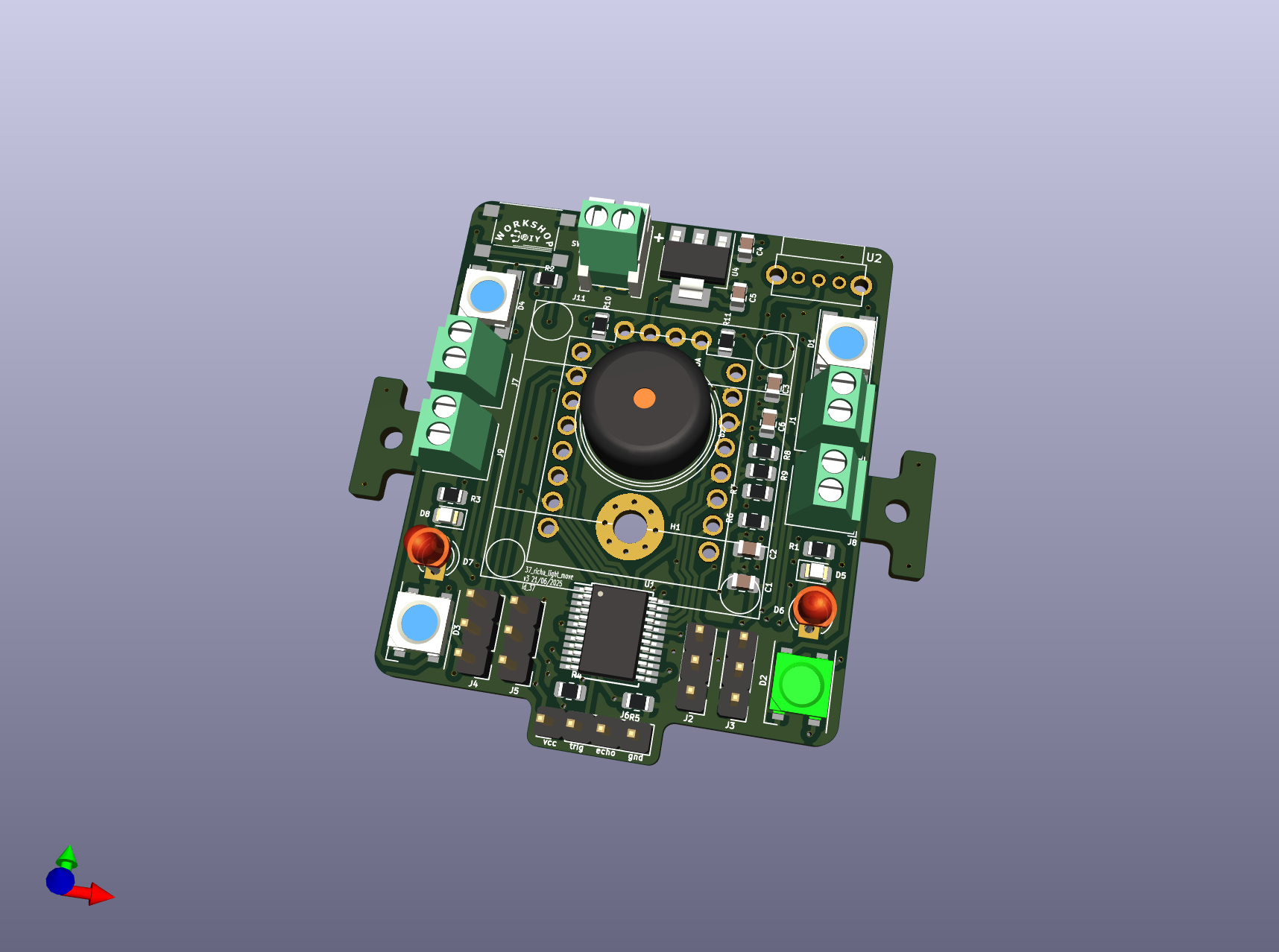
🟫 2 — PCB layer browser
Toggle layers to see what's on each side. Compare with the 3D render above to map silkscreen labels to physical components.
SVGs are rendered to 02_hardware/v3/ by KiCad's File → Plot → SVG. Bundled to Pages by the deploy workflow.
🔌 3 — ESP32-C3 GPIO pin map (from v3 schematic)
All GPIOs as actually wired in the v3 schematic — single source of truth.
| GPIO | Role | Connected to | Direction | Notes |
|---|---|---|---|---|
| GPIO 0 | Push-button input | SW1 (Omron B3F) | IN | 10 kΩ pull-up to 3V3 (R2). Goes via JP1 jumper to GPIO 20 if wanted. |
| GPIO 1 | Motor A direction 1 | TB6612FNG AIN1 + J2 conn + LEDs D5/D6 | OUT | Also drives green status LED pair via 1 kΩ. |
| GPIO 2 | Motor A direction 2 | TB6612FNG AIN2 | OUT | Forms the AIN1/AIN2 truth-table for motor A direction. |
| GPIO 3 | Motor A speed (PWM) | TB6612FNG PWMA + also exposed on J3 | OUT | GPIO 3 always drives PWMA. The J3 3-pin header taps the same signal so an external device (e.g. servo) can share it. Solder jumper JP2 selects J3's power pin: VCC direct (battery) or 5 V regulated (per the 2025-06-21 schematic note). |
| GPIO 4 | Buzzer | R7 → transistor → bz1/bz2 | OUT | Transistor stage (R7 base, R8 series, R9 pull-down). Allows louder volume + protects GPIO. |
| GPIO 5 | Onboard NeoPixel chain | D1 → D2 → D3 → D4 (TX1812, 5050) | OUT | 4× WS2812-compatible addressable RGB LEDs daisy-chained. DIN of D1 = GPIO 5; DOUT of each feeds DIN of next. Drives the "rich light" animations via RMT @ 800 kHz. |
| GPIO 6 | Motor B direction 1 | TB6612FNG BIN1 + J4 conn | OUT | Also routed to J4 servo header (3-pin V+/GND/sig). |
| GPIO 7 | Motor B direction 2 | TB6612FNG BIN2 | OUT | Forms the BIN1/BIN2 truth-table for motor B direction. |
| GPIO 8 | I²C SDA | OLED 128×32 | I/O | 10 kΩ pull-up to 3V3 (R10). |
| GPIO 9 | I²C SCL | OLED 128×32 | OUT | 10 kΩ pull-up to 3V3 (R11). Also BOOT button — pull-up keeps it high at boot. |
| GPIO 10 | Motor B speed (PWM) | TB6612FNG PWMB + J5 conn + LEDs D7/D8 | OUT | Also drives blue status LED pair + J5 servo header. |
| GPIO 20 | Expansion | J7 (2-pin) + JP1 | I/O | JP1 jumper bridges this to GPIO 0 if SW1 isn't used. |
| GPIO 21 | Expansion | J6 (4-pin) | I/O | 4-pin connector — likely external I²C device or ultrasonic sensor. |
🔗 4 — Connectors — what plugs where
11 connectors on the board. The 3-pin ones follow the standard servo pinout (V+/GND/signal); 2-pin pads are motor outputs; 4-pin is for external I²C / sensor.
J1 2-pin
Auxiliary push-button — wires to GPIO 0 via SW1.
J2 3-pin servo
Servo / LED-pair — signal on GPIO 1. Powers the green LED indicator pair.
J3 3-pin servo
Servo-style header that taps the PWMA signal (GPIO 3). JP2 selects whether the V+ pin is VCC (direct battery) or 5 V (regulated) — see schematic note.
V+ (VCC or 5V via JP2) · GND · GPIO 3 / PWMAJ4 3-pin servo
Servo header — signal on GPIO 6 (also TB6612 BIN1).
J5 3-pin servo
Servo header — signal on GPIO 10 (also TB6612 PWMB + blue LED pair).
J6 4-pin · HC-SR04
Ultrasonic distance sensor header. PCB silkscreen labels the four pads vcc · trig · echo · gnd — drop-in for a standard HC-SR04 module.
J7 2-pin
Generic expansion — GPIO 20 + GND. Bridged to GPIO 0 via JP1 if needed.
J8 2-pin pads
Motor A output — TB6612FNG AO1/AO2. Solder DC motor leads here.
AO1 · AO2J9 2-pin pads
Motor B output — TB6612FNG BO1/BO2. Solder second DC motor here.
BO1 · BO2J10 / J11 2-pin
Battery / power input + switched power-out. SK12D07VG4 slide switch (U2) routes between them.
BB1 4-pin I²C
OLED 128×32 — SSD1306-class display module. Inline I²C with R10/R11 pull-ups.
SDA · SCL · VCC · GND🧩 5 — Key ICs on the board
| Ref | Part | Role | Why |
|---|---|---|---|
| U3 | ESP32-C3 SuperMini | MCU | RISC-V 32-bit · WiFi + BLE · USB-C native CDC · 4 MB flash · 13 GPIOs broken out. |
| U1 | TB6612FNG | Dual H-bridge motor driver | Drives 2 DC motors up to 1.2 A continuous each. PWMA + AIN1/2 (motor A), PWMB + BIN1/2 (motor B), STBY enable. |
| U4 | AMS1117-5.0 | 5 V LDO regulator | Steps battery (VDDA) down to 5 V for servos & logic. C4 + C5 = 100 nF decoupling. |
| U2 | SK12D07VG4 | Slide switch (SPDT) | Power on/off — selects between battery and disconnected. |
| SW1 | B3F (Omron) | Tactile push-button | User input on GPIO 0. Pulled high by R2 (10 kΩ). |
| BB1 | OLED 128×32 | I²C display module | SSD1306-class. Status / battery % / sensor readout. |
📝 6 — Schematic revision notes
The bottom-right of the v3 schematic carries two annotated revision notes from the designer:
→ Implication: if you connect a servo via J3 (which shares GPIO 3 with motor PWMA via JP2), the back-EMF can damage the GPIO. Add a
1N4148 reverse-biased between signal and ground.
→ Implication: SG90-class servos draw a stall current spike (~600 mA each). Without bulk capacitance the 5 V rail dips and the C3 browns out. A single 1000 µF electrolytic across 5V↔GND near the servo headers solves it.
KiCad source on GitHub: 02_hardware/v3/ · Other guides: user · build · instructor · learn · start-here